The goal of this project was to learn about the design process for making a power converter. It was the focus of a Masters level Power Design Lab course. For this project we had to design a converter to take 120 VAC and provide a current controlled 20-30 VDC to a load. We completed all parts of the design process: choosing a power converter topology, calculating and building the magnetic inductor, circuit design and simulation, control-loop analysis, component selection, PCB layout and assembly, and testing and verification.
Control Loop
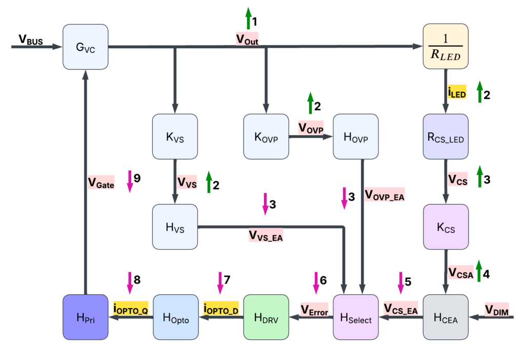
While the LED Driver is primarily current-controlled, it also has an Over Voltage Protection control loop and a Minimum Voltage control loop.
Current-Control
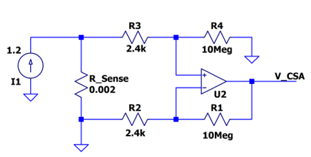
The Current Sense Regulation is the primary Control Loop. It will be running the majority of the time.
In this circuit, we are planning on using a WSK12162L000FEA, sense resistor. However, the differential voltage across RSense may be small enough that it falls victim to noise. In that case, we will have to use a larger RSense resistor, which will necessitate changing the gain on the amplification circuit.
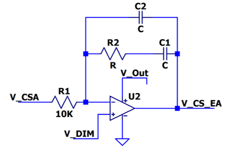
The Error Compensator stage for the Current-Sense loop compares the Current Sense Amplifier signal with the control signal VDim and produces an error signal. The error signal isn’t a level, but an inverted slope whose steepeness is define by the distance betwen VCSA and VDIM, and whose level is a function of how long the error persists.
Minimum Voltage Protection

In order to ensure that the secondary side control sensing is able to operate continuously, we ensure that the is always a minimum voltage on the secondary side VBus. In order to accomplish this, we use a measure VBus using a voltage divider, and compare it to a chosen VRef. When the voltage is above VRef, the error signal trends downward until it rails, and is ignored by the signal selector. However, as VBus approaches VRef the error signal’s slope decreases, and then increases as VBus goes below the threshold. At this point, the error signal gains priority in the signal selector, and keeps VBus at the minimum voltage regardless of the current setting.
PCB Layout
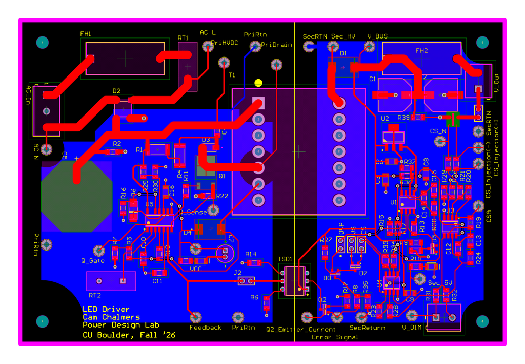
After designing the schematic and selecting components, I laid out the PCB. Because of the high currents and high di/dt of the switching, I paid special attention to several layout aspects. I separated the input and output stages to keep them isolated. I attempted to keep the power and signal portions of each stage separated to reduce the impact of EMI noise on the control loops. I kept the current loops as small as possible to minimize the parasitic inductances. I kept current-carrying traces at 100 mils wherever possible. I used creepage and clearance rules to ensure no arcs or shorts between current-carrying traces.